


Capacitor types
The number of capacitor types is even greater than the number of resistor types. The differences are large and based on a large number of parameters.
Some of the most commonly used capacitors are discussed here. A more detailed discussion can be found here:
https://nl.wikipedia.org/wiki/Condensator
and here:
https://en.wikipedia.org/wiki/Ceramic_capacitor#Multi-layer_ceramic_capacitors_.28MLCC.29
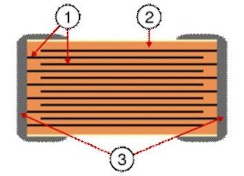
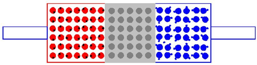
MLCC
The multi-layer ceramic capacitor is currently the most commonly used capacitor in electronics. These capacitors are stable, small and are not affected by LR components. However, in general they are only suitable for low voltages. The dielectric (2) consists of an extremely thin ceramic film. The plates of the capacitor (1) consist of a vapor-deposited layer of metal. The plates are connected alternately to the connection caps (3), creating a multi-layer stacked capacitor.
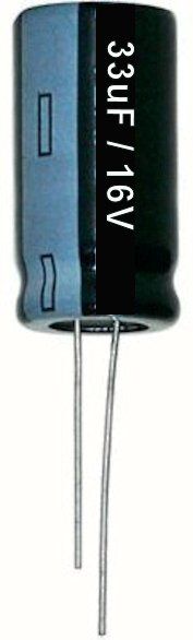
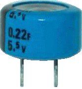
The electrolytic capacitor
This capacitor, also called an electrolytic capacitor, is specially designed for large capacities.
It consists of two rolled (for large surface) layers of aluminum foil separated by paper or porous plastic, soaked in an electrolyte. The electrolyte makes the paper conductive, making it part of one of the "plates." The dielectric is formed by aluminum oxide on one of the two plates. Aluminum oxide is extremely thin, which makes the capacity very high. The disadvantage is that the oxide is maintained by the applied voltage. Electrolytic capacitors are therefore "poled": they have a plus and a minus pole. When the voltage is reversed, the dielectric is broken down quite quickly, after which a short circuit occurs. The electrolyte can explode and the electrolyte is released in gaseous form, which is very harmful to health. That is why this capacitor has its own symbol, which expresses the polarity.
Electrolytic capacitors are usually used as a reservoir capacitor. This means that it can store a large amount of energy that can be extracted at times of scarcity. So you often find it in power supply circuits. An important parameter for these capacitors is the internal resistance that occurs during discharge. For switching power supplies, a low internal resistance of the order of tens of milliohms is very important. The English term for internal resistance is ESR.
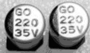
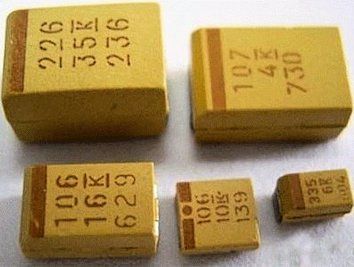
Tantalum electrolytic
The substance tantalum oxide (Ta2O5) is such a good electrolyte that very small surface mounted (SMD) capacitors can be made with a low ESR and a very small leakage current. The voltage is limited to a maximum of 35V. The value ranges from 0.1µF to approximately 100 µF. The tantalum electrolytic capacitor is also sensitive to polarity with short circuit and explosion hazard if incorrectly connected. Tantalum is a rare element and therefore very valuable. Moreover, it is mainly found in areas of Africa where corruption and war are rampant. That is why there has been a feverish search for alternative materials such as Nobium, which can be extracted in larger quantities.
Glass and oil capacitors
These capacitors are used in special circumstances such as high voltages (glass) or high powers (oil). We rarely encounter them in electronics.
Film including polypropylene
The structure of a film capacitor is comparable to that of an MLCC. However, an extremely thin plastic film is used as a dielectric. Just like with MLCC, the plates are connected in parallel to the electrodes, so that there are, as it were, a lot of small capacitors in parallel. As a result, the capacitors have little parasitic inductance, they are very low-impedance and therefore suitable for high frequencies and large peak currents. Polypropylene in particular is extremely stable with almost linear behavior over a wide frequency band. That is why these capacitors are often used in resonance circuits. Polyester as a dielectric has a high stability over a long service life and is a very cheap alternative to Tantalum.
More information can be found here:
https://en.wikipedia.org/wiki/Film_capacitor
Mica
Mica capacitors are produced by evaporating silver onto a mica dielectric. They are expensive precision capacitors with very low leakage current and a high breakdown voltage.
Supercaps
Thanks to special materials and production processes, it is now possible to make relatively small capacitors with a very large capacity. Supercaps up to several thousand kF are produced. In fact, these reservoir capacitors serve as an emergency power supply when another power source fails. In this sense they can be compared to rechargeable batteries, it said that their capacity is still thousands of times smaller than that of a Li-ION cell. However, batteries have the disadvantage that the charging current is limited, so charging takes a very long time. A 3000kF supercap is charged in a few tens of seconds. In terms of lifespan, batteries and supercaps do not differ much (on average 5 years depending on the number of charges and discharges). Supercaps can now only be made for low voltages of 1 to 6 volts.
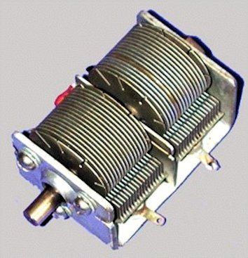
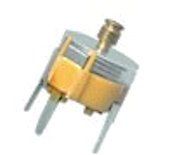
Tuning Capacitors (Air)
A capacitor with air as a dielectric is now a museum piece, but should not be missing. Almost every older radio has a tuning capacitor with air as a dielectric. By turning the shaft, the plate surface of the capacitor is increased or decreased.
There are also very small rotating capacitors called trimmers and toll trimmers,
Nowadays we do not often find them used because they are relatively large and because high-frequency technology has been digitized.
Semiconductor capacitors.
The PN junction in semiconductors always has a capacitive component in the order of a few picofarads to several hundred picofarads. On this basis, a capacitance diode (varicap) has been developed, the value of the capacitance of which can be varied by the reverse voltage applied to the diode.
https://en.wikipedia.org/wiki/Varicap
Applications of capacitors.
Here are the most common applications of capacitors in a row:
- to block direct current but allow alternating current to pass, for example an audio signal to a loudspeaker without direct voltage or the AC/DC switch on an oscilloscope; in frequency filters, for example in audio applications; to smooth out voltage fluctuations, for example in rectifiers; together with coils in vibration circuits for tuning to certain frequencies in radios and many other applications; together with a resistor as a timing element in an integrated circuit such as the NE555 and NE551, in electric clocks, alarm clocks and counters; in the form of a condenser microphone; to detect the position of a conductor to be determined on some touch screens; to absorb and emit electrical energy, such as in the starter motor in a car with a gasoline engine, drive in electric cars, bicycle lights and flashlights with LEDs, where power is supplied for a long time.[source?]to to deliver power in pulses, such as in radar installations, particle accelerators, pulsed lasers, electromagnetic weapons such as the railgun, nuclear weapons detonators, the flash of a camera, and so on. Source Wikipedia
Filter types based on R and C
A filter is (in this context) a circuit that removes frequencies from an offered signal. What is important here is the extent to which the suppression of the unwanted frequencies takes place (slope) and the precision with which this takes place (quality or Q). This depends on the characteristics of the filter. In low-frequency applications, an RC filter is usually sufficient, in high-frequency circuits coils are also used as filter elements. With the filters discussed here, the signal is always weakened.
Depending on the application, the following filters are in use:
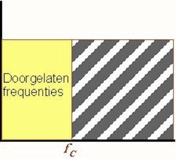
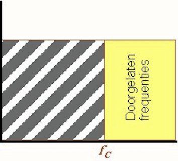
The low-pass filterThe ideal low-pass filter allows all frequencies up to the cut-off frequency fC to pass, while all frequencies above the cut-off frequency are rejected.
The high-pass filter
The ideal high-pass filter allows all frequencies from the cut-off frequency fC to pass, while all frequencies up to the cut-off frequency are rejected.
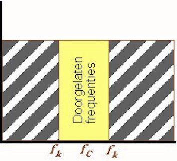
The bandpass filter
The ideal bandpass filter allows all frequencies on either side of the center frequency to the cutoff frequencies to pass, while all frequencies outside the cutoff frequencies are blocked.
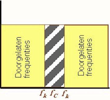
The notch filter
The ideal notch filter is in fact an inverse bandpass filter and therefore allows all frequencies to pass except a defined frequency band.
Filters based on R and C in detail The RC filters discussed below are passive, ie no amplification is applied. The final result is therefore always an attenuation of the input signal. Moreover, the filters do not meet the ideal picture as shown above. The characteristic will be a slow falling or rising line from the center frequency.
Because there is only one frequency-dependent element in the circuit, we call them first order filters. The cut-off frequency is called the frequency at which the filter reaches an attenuation of -3db.
The different filters are now discussed in detail. We call the input signal VIN and the output signal VOUT.
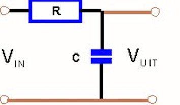
The operation of the low-pass filter
The impedance of the capacitor decreases with increasing frequency. At low frequencies the impedance is high, at high frequencies the impedance is low. (impedance is also called alternating current resistance) The resistance is the same for all frequencies. The formulas are now simple to derive.
Suppose C is actually an (alternating current) resistor, then the formula for the voltage divider applies:
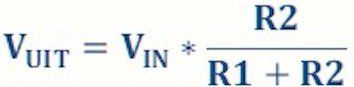
R2 = then the alternating current resistance of the capacitor, so RC. The total resistance is the sum of both resistances: RS = R1 RC
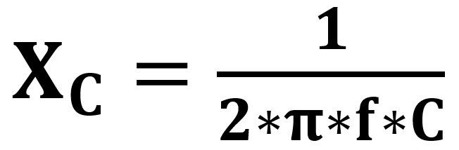
The resistance of the capacitor is given by:
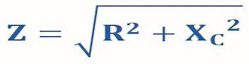
The total resistance is therefore also frequency dependent! It is represented by Z:
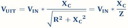
By now entering this result into the series resistance formula, we arrive at the output voltage:
A comment regarding the damping of the filter is appropriate here. The calculations and the bode diagram shown below assume ideal components without load. In practice, those ideal components do not exist! Capacitors have a small ohmic series resistance and a very high parallel resistance. Large capacitors have a parasitic coil on board even at high frequencies. The effects are generally small but can play a major role in critical circuits. Finally, the output of a filter is always connected to the input of a subsequent circuit, which therefore loads the output. As a result, there will be an attenuation of the signal in any case, which depends on the input resistance of the next circuit.
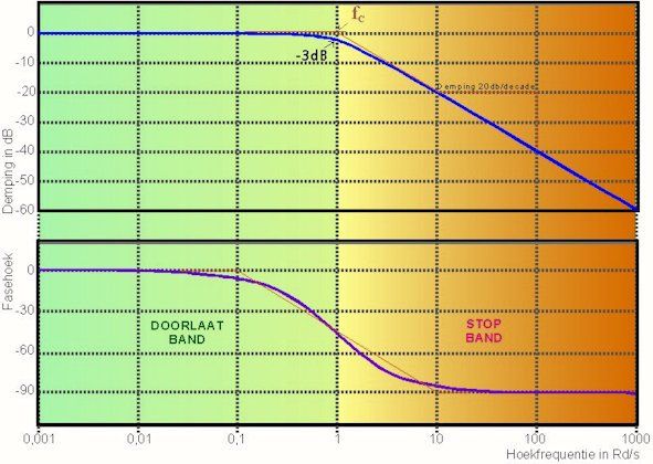
The Bode diagramThe behavior of an RC filter can be represented graphically using a Bode diagram. Such a diagram allows you to understand at a glance the behavior of the represented RC filter. An example of a Bode diagram of the low-pass filter is shown below.
The frequency response is shown in the upper part of the diagram. The characteristic runs horizontally until close to the cut-off frequency. Then it bends down to reach the cutoff frequency at -3dB. The characteristic then bends further to an attenuation angle of 20dB per decade or 6dB per octave. The area from 0 to the cut-off frequency is called the passband and is also the bandwidth of this filter.
The area above the cutoff frequency is called the stop band. The attenuation in the stop band increases with frequency and very high frequencies will no longer be allowed through at all.
The cutoff frequency is the frequency at which the AC resistance of the capacitor is equal to the ohmic resistance of R. That is the point at which the attenuation is -3dB and the output voltage is 70.7% of the input voltage. That seems strange because the two resistances are the same, right? Please note that the sum of the resistances is also frequency dependent. Z will therefore also change dynamically. The calculation can be checked using the included spreadsheet.
The lower part of the bode diagram shows the phase behavior of the low pass filter. At low frequencies, the AC resistance of C1 is very high and has little influence on the output signal. The circuit behaves resistively (like a resistor) and therefore there is no phase shift. As the frequency increases, the alternating current resistance of C decreases and the phase behavior will be increasingly influenced by C.
The phase angle M of the output signal with respect to the input signal becomes increasingly larger. At the cutoff frequency M al is -45o . The output signal lags behind the input signal due to the charging time of the capacitor.
Ultimately, the alternating current resistance of the capacitor becomes so small that it completely dominates the circuit. The phase angle M has then become 90°.
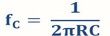
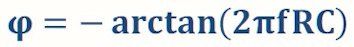
The crossover frequency and phase angle can be calculated as follows:
Cutoff frequency:
Phase angle:
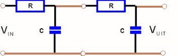
Multiple order RC filters
A disadvantage of the filters discussed above is the attenuation angle of 6dB per octave. We often want to transmit a specific frequency range very precisely. The answer seems simple. We simply place two or more low-pass filters in a row.
This way we can combine filters. Depending on the number of frequency-dependent elements, they are given an order number. Two low-pass filters in succession form a second order filter.
The number of n filters in a row forms an nth order filter. We can simply calculate the attenuation angle by multiplying n by -20dB. An nth order filter therefore has an attenuation of
n x-20dB/decade or nx6dB/octave. In this way, a 4th order filter comes close to the ideal characteristic of a low-pass filter. Unfortunately, practice is more difficult. After all, each filter places a (frequency-dependent) burden on its predecessor! The results for output voltage and cutoff frequency are dramatic. With each filter, the output voltage at the cutoff frequency is approximately 70% of the signal of the predecessor. With a 4th order filter you are left with 0.7*0.7*0.7*0.7*VIN, which is equal to approximately 24% of the original input signal! The official formula for the attenuation of an nth order filter is as follows:
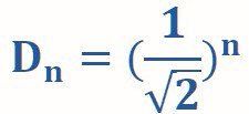
Where 1/V2 is approximately equal to 0.707.
Because the load on each filter stage is a frequency-dependent filter stage, the cut-off frequency depends on the combined filter stages:
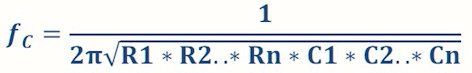
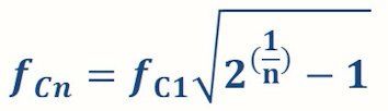
With the number of filters, the cut-off frequency also shifts downwards according to the following formula:
The results are clearly visible in the bode diagram of a 2nd order low-pass filter:
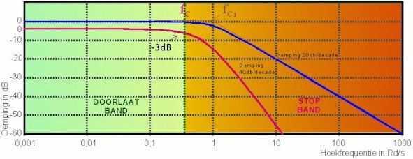
The blue line is the characteristic of a first order low-pass filter, the red is the characteristic of a second order low-pass filter based on the same components. Due to the mutual dynamic coherence, it is difficult to design and apply a stable multi-order filter. As a rule of thumb, the resistor is 10x larger and the capacitor 10x smaller in each subsequent stage. This of course changes the Fc of filter 2, which largely negates its effectiveness.
Multiple order filters are therefore generally designed as active filters using one or more operational amplifiers.
SEMICONDUCTORS
What actually is a semiconductor?
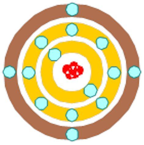
In the 1950s people started experimenting with substances that we now call semiconductors. To understand what is meant by a semiconductor, we take a trip to physics and namely Bohr's atomic model. Here the atom is depicted as a positive nucleus around which negative electrons circle in fixed distances (shells) from the nucleus
The smaller the shell, the fewer electrons fit in it. The first shell can only contain 2 electrons, the second 8, the third 18 and all higher shells 32. The most stable configuration for an atom is that the outer shell is full.
If we now look at the most commonly used semiconductor material Silicon, we see that Silicon has 14 electrons. That is, 2 8 4
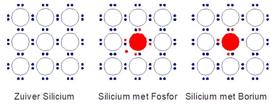
Above you see a crystal lattice of silicon in the first picture. It is a strong lattice because the silicon atoms can always borrow an electron from each other to complete the outer shell. You actually have to imagine the picture in three dimensions. The six pairs are therefore always shared by two atoms. This makes the bond between the electrons and the nuclei very strong (this is called covalent bonding). Pure silicon is therefore a poor conductor. If we contaminate the pure silicon with atoms that do not fit exactly into this lattice, such as phosphorus that has 5 electrons in the outer shell, a phenomenon arises that we can make good use of. The one remaining electron of the phosphorus atom does not fit into the bonds and is therefore “free”. This greatly increases the conductive properties of the crystal. Because there are “too many” negative particles in this lattice, we call it N-Silicon. We can also apply a contamination with an atom with three electrons in the outer shell, such as Boron. Now a hole is created, as it were, in the lattice into which an electron can easily insert. However, that electron then comes from another atom, which in turn has an electron shortage. In this way, the hole, as it were, moves through the material, making it conductive. Silicon with this contamination is called P-Silicon.
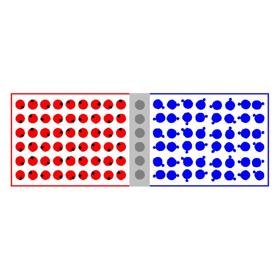
What happens if we stick a slice of N-Silicon against a slice of P-Silicon? After all, the N-Silicon contains “free” electrons and the P-Silicon “free” holes? Although both materials are neutral, the holes in the P material attract electrons from the N material. The holes in the contact layer are filled by the electrons. As a result, there are no free holes or electrons in the contact layer. This completely filled layer closes the passage for the other electrons (or holes). The wafer-thin layer (of the order of a thousandth of a millimeter) is therefore called the barrier layer.
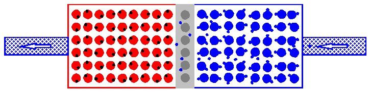
If we now squeeze electrons into the N layer of the diode, the pressure on the barrier layer increases. At a certain point the pressure (voltage) is so great that the electrons can jump over the barrier layer. Above that voltage (0.7 Vol with ordinary silicon) the diode conducts almost completely. With an unlimited voltage source this will lead to very high currents, causing the diode to fail. A series resistor is therefore necessary
If we squeeze electrons into the P layer of the diode, they will fill the holes in this layer and the barrier layer will therefore become wider. (the same happens on the N side where we actually suck away the electrons) The result is that no current flows at all. (in reality, almost every diode has a very small leakage current). Please note that this behavior is subject to a maximum voltage. If exceeded, the diode will break.
The Mosfet as a switch.
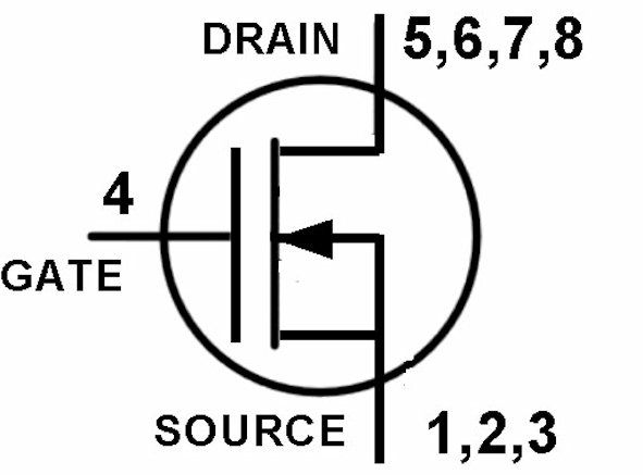
A Mosfet is very suitable as a switch for high currents and voltages. Now that the prices of Mosfets have dropped to the point where they are approaching a transistor, the Mosfet is the best choice when you need a DC switch. Just to repeat: the Mosfet has three connections, Drain, Gate and Source. There are of course two versions, called N-channel and P-channel. For an explanation of the P version, you simply need to mirror all values. The Mosfet is best regarded as a voltage-controlled current source. A technically extensive treatment of the different types of FETs can be found here.
Before you start with the circuit, it is good to first think about how much DC voltage and current need to be switched. Based on that information you can select the right mosfet. The most important parameters can be found in the manufacturer's data sheets. This concerns the drain current ID, the gate voltage VGS, the maximum drain voltage VDS(MAX) and the maximum power that the mosfet is allowed to dissipate. An important parameter is the conduction resistance at full conduction RDS(ON). Furthermore, the minimum gate voltage at which the mosfet starts to conduct VGS(th) is important. The Drain behaves more or less like a current source that, from a volt or two of drain voltage, supplies a constant current whose magnitude depends on the gate voltage. The gate is completely isolated from the rest of the Mosfet and therefore no gate current flows! This makes a Mosfet very easy to control with a DC voltage. However, the Mosfet has a relatively large surface area with a very thin separating layer between the Gate and the substrate. As a result, the Mosfet has a relatively large input capacity. This ensures that current flows briefly to the gate to charge it (see capacitor). That short peak can be so intense that it is sometimes necessary to protect the control circuit with a series resistor in the gate line, which makes the switch somewhat slow. NOTE Because MOSFETs behave like an adjustable current source, the highest current or lowest internal resistance is usually only achieved at a voltage that is considerably higher than the VGS(th)
Usually even a voltage that is higher than the 5V that a 5V microcontroller supplies as logic 1. So you have to carefully read the data sheets to see whether the mosfet can supply sufficient current at the logic voltage that your system supplies. (see here) An alternative is to choose a mosfet designed to work with 5V logic. That's called a logical mosfet. In that case, the data sheets state a continuity resistance RDS(ON) at 5 Volt and a starting voltage VGS(th) of 0.5 to 1V
This problem becomes even greater with 3.3V logic, but fortunately there are solutions available here too. For example, the IRLZ44 and the Si4866DY already work well at the gate voltage of 3.3V and can therefore be directly used for switching large DC currents in a 3.3V system. If you already have a mosfet available that does not meet these "logical" requirements, you can easily build an auxiliary circuit yourself. You can find an extensive discussion on this subject here.
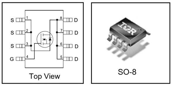
For clarity, the connections of the IRF7470PbF
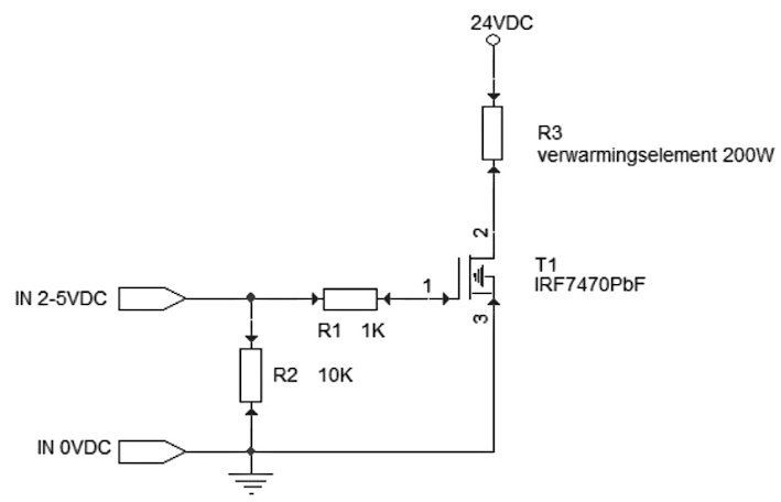
As an example, a switch for a 24V 200W heating element.
The heating element is a wire resistor with a small inductance. That is why no freewheeling diode is included. Because the resistance of the heating element is lower during a cold start, we must take into account at least 5 amps of starting current. The chosen Mosfet IRF7470PbF does this job very quickly: VDS(MAX) =40V, ID(MAX) =10 A, power 2.5Watt at room temperature, RDS(ON) = 13 mOhm (0.0013 ohm) and a VGS( th) of 2 Volts. Please note that the lowest resistance and high current are only achieved at a high Gate voltage, in this case 4.5 V. As an example, a switch for a 24V 200W heating element.
The heating element is a wire resistor with a small inductance. That is why no freewheeling diode is included. Because the resistance is lower during a cold start, we must take into account at least 5 amps of starting current. The chosen Mosfet IRF7470PbF does this job very quickly, the maximum power of 2.5 Watt at room temperature is far from being achieved. The Mosfet has an input capacitance of 5 nF. The 1K series resistor protects the control against high current peaks. The 10k resistor ensures that the control voltage is always at zero volts without active control.
The transistor as a switch.
If you want to switch larger currents and/or voltages, for example with an Arduino, the transistor is a good solution. The transistor is one of the most commonly used applications for this purpose, it is cheap and easy to use.
Just to repeat: the transistor has three connections, Collector, base and emitter.
There are two versions, an NPN and a PNP version. The NPN version is discussed here. For an explanation of the PNP version, you simply need to mirror all the values.
Before you start with the circuit, it is good to first think about how much DC voltage and current need to be switched. Based on that information you can select the right transistor. The most important parameters for this can be found in the manufacturer's data sheets. The maximum values and the normal "in operation" values are given for the collector current IC, the base current IB and the voltage across the transistor VCE. Furthermore, VBE max and the maximum power IC*VCE are also specified. Finally, the current amplification factor HFE (ß) is an important value. With an NPN transistor, the collector (via the load) is connected to the positive voltage, while the emitter is connected to zero. The collector must always be more positive than the emitter! In that case, the collector is the base current times the current gain factor. In formula form: IC = HFE*IB = ß*IB. The base current and the collector current together form the emitter current. Please note that the HFE differs per transistor of the same type and also depends on the collector current, the voltage across the emitter and the temperature. Fortunately, this does not make much difference for the transistor as a switch, we always choose the base current on the large side to guarantee fast and reliable switching. Furthermore, the following recommendations. Also ground the base with greater resistance so that the base is always defined. Protect the transistor against spikes by inductive loads (relays) with a freewheeling diode. This of course also applies to any negative voltage peaks!
Vezadiging
Something else happens due to the higher base current. In principle you also expect a larger collector current, but a transistor cannot work if the collector voltage is not greater than the emitter voltage. Due to the larger base current, the transistor now searches for the point at which it still functions properly. This means that there remains a voltage across the collector/emitter of 0.5V or even less. The transistor is in saturation! And that also limits the dissipation of the transistor, which is now 0.5 x 0.033 = 0.0165 mW, so it is smaller than 20mW, which is well within the specifications of the transistors mentioned.
As an example, a switch for a 12V relay.
The relay in this example is the Panasonic DS1MNil12 with a coil resistance of 360 ohms and a current of 33.3 mA. This relay is even able to switch 230VAC, but at a small current. At 30VDC the relay switches 2 A.
All transistors mentioned can carry well more than 33.3 mA. The transistor is protected against voltage peaks across the coil by the diode D1.
Now let's do the math, the BS 546B has an HFE of 150, so for the 33 mA collector current a base current of 33/150 = 0.22 mA is needed.
Assuming that the control voltage on the input is 5V (Arduino), then the base current is (5-0.7)/2200=2mA. So a factor of 10 too large. The 0.2 mA current via the pull-down resistor is negligibly small. The factor 10 is fine in this case. Firstly, because the HFE of the transistor becomes much smaller with a small voltage difference between collector and emitter. Furthermore, components that require a higher starting current can also be switched in this way.
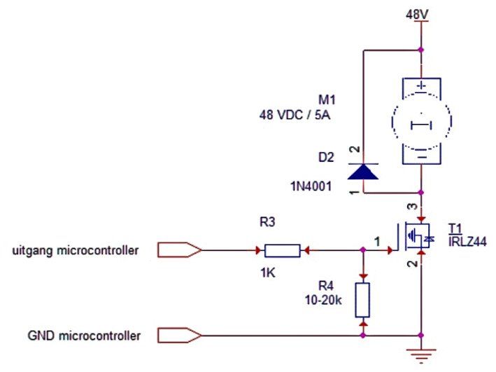
If you want to switch higher voltages and/or currents, you will quickly encounter problems, such as a high required base current and/or a high saturation voltage, i.e. too much power. In that case it is more convenient to choose a mosfet. Therefore an example of a mosfet switch. Example 2, a 48 VDC / 5 A motor connected with the mosfet IRLZ44
The IRLZ44 is a “logical mosfet”, which means that it can switch well based on the logical voltages 0 VDC and 5 VDC. And even with a 3.3 VDC system, the MOSFET still works fine. With an internal resistance of 0.05 ohms, the power is also limited to 250 mW at 5 A. The 1K resistor is intended to protect the output of the controller against the charging peak of the gate capacitor of 3.3nF. R4 is a guarantee that the mosfet always switches off when the controller is not active.
Resistance types
There are so many variations of resistors that it is impossible to discuss them all in detail.
But there are a number of main groups whose general properties can be discussed well. This classification is made on the basis of the resistant material with which the resistance is built up.
In this way we can name 4 groups:
1. Carbon
2. Metal oxide film (cermet)
3. Wire wound
4. Semiconductor material
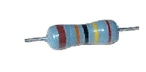
Carbon
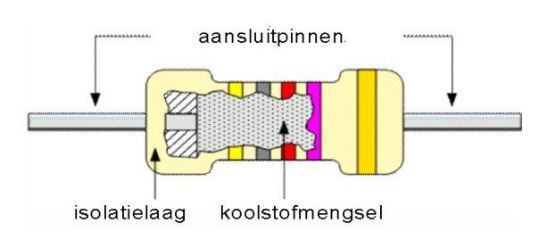
This cheap and widely used technique involves mixing conductive carbon with a non-conductive ceramic powder.
The mixing ratio determines the resistance. The assembly is provided with a connecting pin at both ends and provided with an insulating (and sometimes fire-inhibiting) lacquer with the resistance indication in circles on the housing.
Due to its low inductance, the carbon resistor is suitable for high-frequency applications. A disadvantage of the carbon resistor is the high noise contribution, especially at higher temperatures. The power range runs from a few milliwatts to 5 watts. The greater the power, the greater the dimensions of the resistor, of course. Making resistors with high precision values is more difficult with this technique. Therefore, carbon resistors generally have a high tolerance.
Film resistance
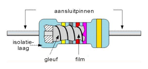
With a film resistor, a low-resistance material is vaporized on a ceramic carrier. The properties of the film resistance are partly determined by the material used. Uses include pure metals such as nickel, oxides such as tin oxide and carbon.
The value is partly determined by the thickness of the vapor-deposited layer. By later cutting a spiral in the vapor-deposited layer with a laser, very high-precision resistors can be made with a tolerance of 0.001%. The disadvantage of the method is that it increases the inductance of the resistor.
Metal film resistors have higher temperature stability and a much lower noise factor than carbon resistors. However, they are less good at handling peak flows.
Cermet resistors
The thick film resistors have an even lower noise factor. In these resistors, the layer of vapor-deposited material consists of a mixture of ceramic material and a metal.
Film resistors have a limited power range from a few milliwatts to about ½ watt.
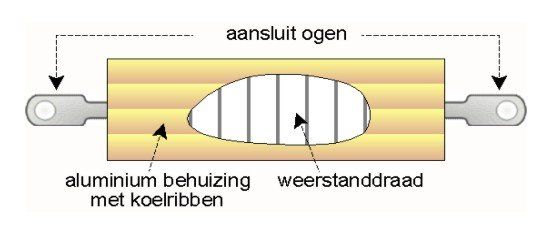
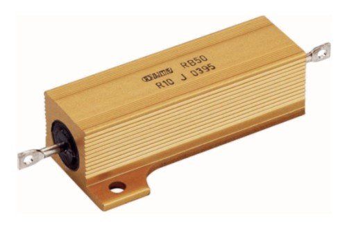
Wirewound resistors
A wirewound resistor is made by wrapping a wire of resistance material around a ceramic carrier. The wire consists of an alloy with a defined resistance. In this way, resistors can be made from very small values up to several hundred kilo ohms. Wire resistors can withstand high peak currents and can be cooled well, making them suitable for large powers of up to hundreds of watts. Unfortunately, because they are wound, they have inductive properties that make them unsuitable for higher frequencies.
The resistors for higher powers are placed in a housing that can dissipate heat well. This can often be mounted on a larger heat-dissipating surface.
When using wire-wound resistors in alternating current circuits, the inductive reactance of the resistor must be taken into account.
This inductive reactance must, as it were, be added to the DC resistance indicated on the resistor. The correct formula for calculating the impedance or alternating current resistance of the wirewound resistor is a little more complicated:
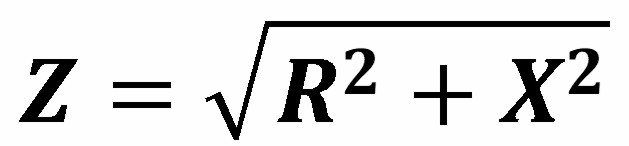

Where Z is the total impedance, R is the DC resistance and X is the inductive reactance.
Since the inductive reactance depends on the frequency of the signal (XL =2πfL), the resistance therefore changes depending on the frequency. This makes wirewound resistors unsuitable for alternating current applications with variable frequency.
Special winding techniques have been developed that can also be used to make low-induction wire resistors (bifilar winding).
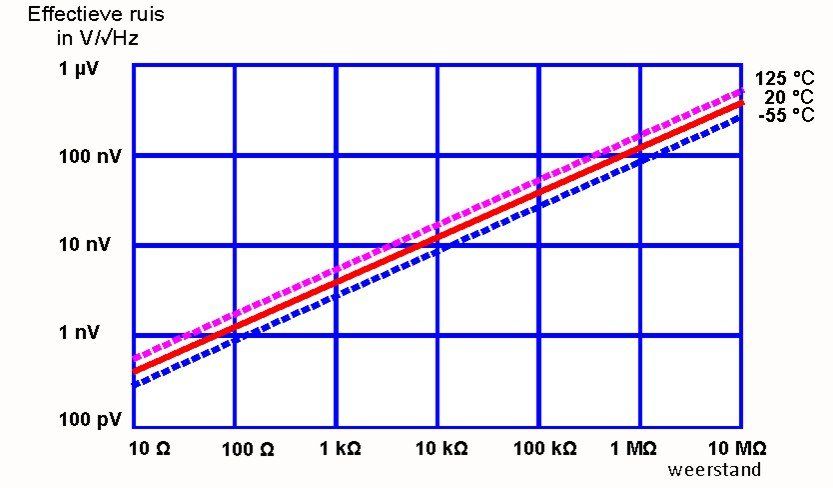
Russia
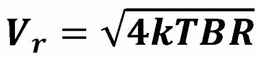
A resistor contains relatively many free electrons. The movement of those electrons reveals itself in noise, called Johnson or thermal noise. The higher the temperature, the greater the mobility of the electrons and the more noise a resistor produces.
The noise produced is evenly distributed over the entire spectrum and is called white noise. The Thevenin model of a noisy resistor consists of a clean resistor in series with a noise generator.
The noise is proportional to the square root of the product of the bandwidth B in Hz, the temperature T in kelvin and the resistance R in ohms:
K represents Boltzman's constant (1.38.e-23).
Semiconductor “resistors”
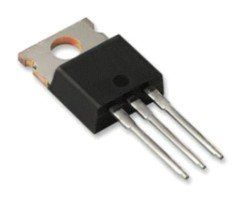
Semiconductors such as transistors can be used as resistors. Power transistors usually have a heat sink that can be mounted on a larger cooling surface, allowing them to handle very high powers. With the help of some added components, voltage regulators and current sources can be made with excellent properties. Voltage regulators (linear) are available completely integrated for a wide range of output voltages. The output voltage is no longer dependent on the load (within the limits of the specifications, of course).
The example shown here is an L7812CV from ST. The IC provides an output voltage of 12 volts at a maximum current of 1.5 amperes and a maximum input voltage of 35V. The useful thing about these types of ICs is that they are (usually) also current and temperature limited so that they do not break in the event of a short circuit. A disadvantage is that these circuits only work with DC voltage.
Maximum power point
MPPT is commonly used for solar panels, windmills and watermills.
MPPT stands for maximum power point tracking, which means that you ensure that the generator is always adjusted so that it delivers maximum power.
That is not very obvious.
Take a look at the graph below for a single cell of a solar panel.
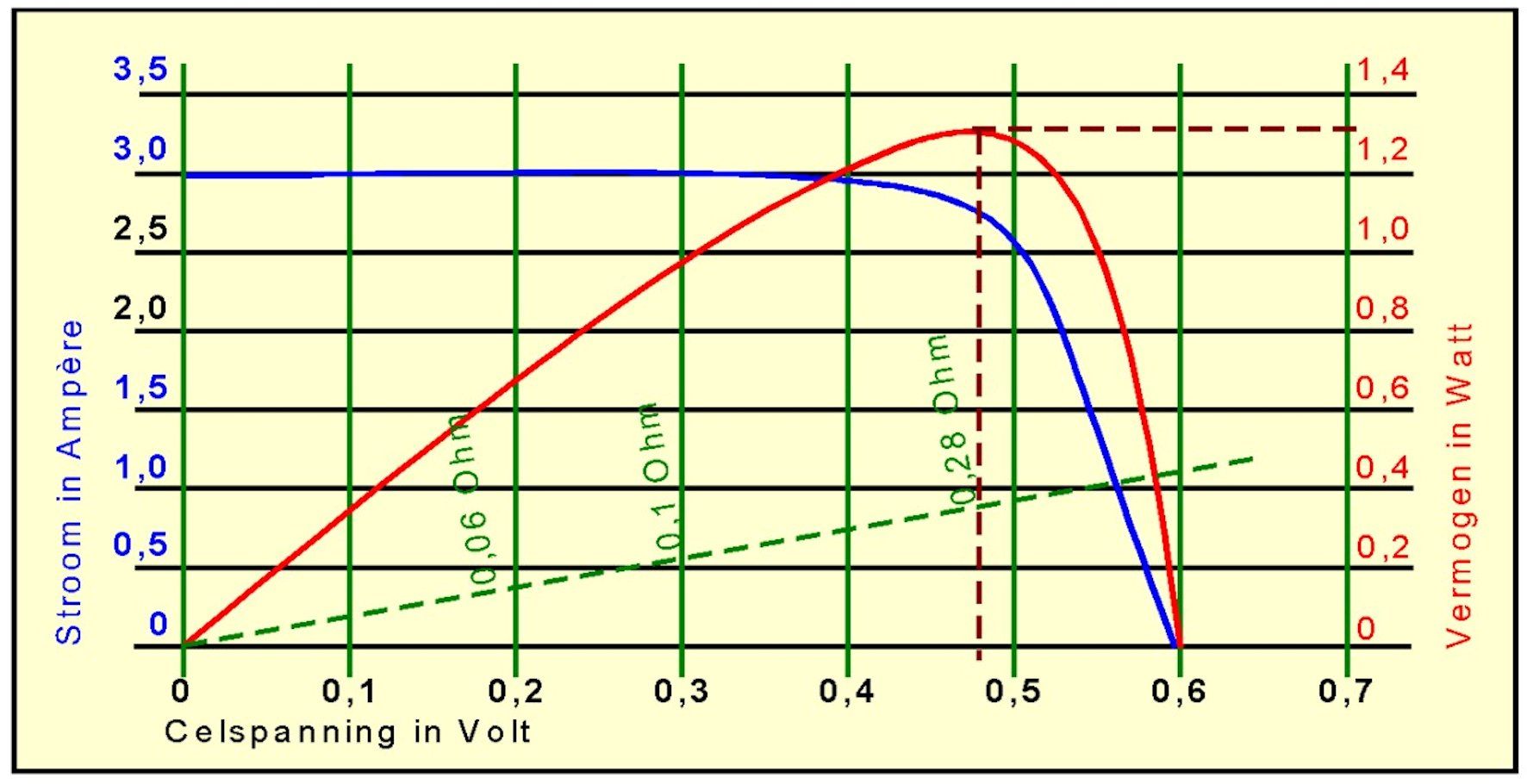
We assume that this cell is optimally illuminated by the sun.
The cell then supplies a current of approximately 3 amperes. If we put a heavy load on the cell, for example with a resistance of 0.06 Ohm, the cell can only supply 0.18 Volt and therefore a power of only 0.4 Watt. At 0.1 Ohm the yield is already better by almost 1 Watt.
At 0.28 Ohm the maximum output is 1.3 Watt at 0.48V and 2.7 Ampere.
With higher resistance, the current decreases to such an extent that the delivered power quickly decreases. So there is exactly one load that gives the best result with regard to the power supplied. And that load does not only differ per cell, but also with the amount of light that falls on the cell. And the same applies to a wind or water turbine-driven generator. That is why the maximum power point is always monitored and the load is constantly adjusted accordingly. That's called maximum power point tracking.
In good Dutch, continuous optimization of the tax.